PCB & Electronics
High-speed, multilayer, EMI-optimised PCB design ready for manufacturing. From schematic to fabrication files, we engineer electronics that work.

Common Challenges in PCB & Electronics Design
Signal integrity failures, EMI issues, and DFM problems are among the most common reasons hardware products miss their launch window. Poor PCB design decisions made early create expensive respins later.
Unvalidated Product Ideas
Ideas move forward without technical or market feasibility analysis, resulting in impractical designs and wasted investment.
Design Without Manufacturing Alignment
Products designed without considering assembly, materials, and tooling constraints often face expensive redesigns later.
Weak Industrial Design
Poor ergonomics, material selection, or usability planning can reduce product appeal and market acceptance.
Our Approach
From idea to production — delivered through a clear, structured process.
Schematic Capture
We translate your circuit requirements into a clean, reviewable schematic ready for peer review.
PCB Layout & Routing
Our engineers perform high-speed routing, impedance control, and EMI mitigation strategies.

Design Rule Check & Review
Automated DRC followed by a thorough manual review catches issues before fabrication.
Fabrication & Assembly Handoff
Complete Gerber, BOM, and assembly files delivered for a smooth manufacturing transition.
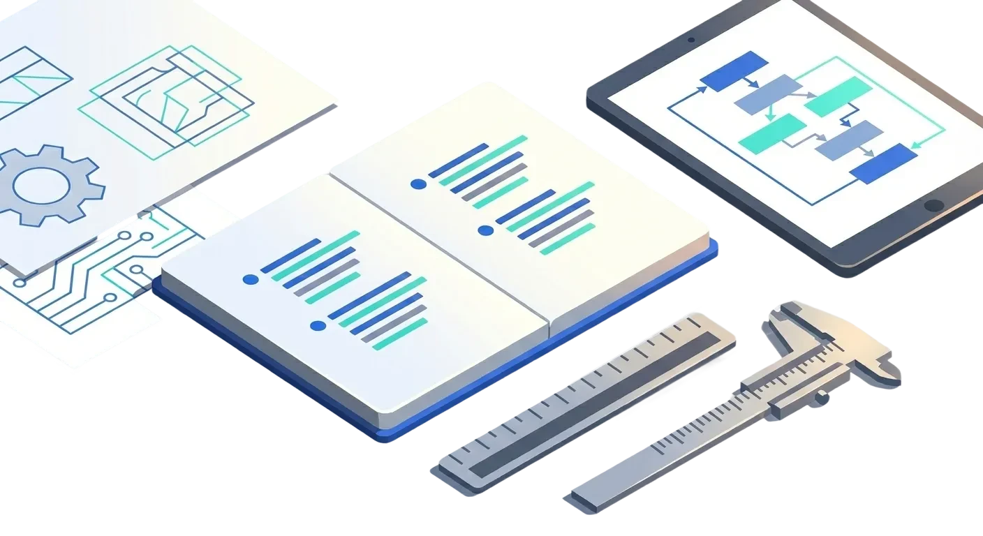
Technologies & Tools
From early feasibility to production-ready design, we ensure every concept is technically validated and manufacturing-aligned.
Capabilities
From early feasibility to production-ready design, we ensure every concept is technically validated and manufacturing-aligned.
High-Speed PCB Design
Multi-gigabit signal routing with controlled impedance, differential pairs, and length matching for reliable high-speed performance.
Power Electronics
Custom power supply design, DC-DC converters, battery management, and power sequencing for efficient, stable power delivery.
RF & Wireless Design
Antenna design, RF front-end circuits, and wireless module integration for Bluetooth, Wi-Fi, LoRa, and cellular applications.
EMI/EMC Engineering
Noise mitigation, filtering, shielding, and layout strategies to ensure your product passes regulatory testing first time.
Multilayer Stack-Up Design
Optimised layer stack-ups for signal integrity, power distribution, and thermal performance across complex multilayer boards.
BOM & DFM Optimisation
Comprehensive bill-of-materials management, component qualification, and design-for-manufacturing reviews to reduce cost and risk.
Case Studies
Proven Execution Across Complex Hardware Projects.
Designed and scaled a rugged IoT gateway with optimized BOM and remote update capability.

Delivered low-power PCB and firmware architecture for continuous monitoring.
Integrated AI accelerator with optimized power and heat management.

Designed and scaled a rugged defence module with optimized BOM and remote update capability.
Designed and scaled a rugged IoT gateway with optimized BOM and remote update capability.
Delivered low-power PCB and firmware architecture for continuous monitoring.
Integrated AI accelerator with optimized power and heat management.
Designed and scaled a rugged defence module with optimized BOM and remote update capability.
Yes. Our engineers are experienced with DDR, PCIe, USB 3.x, Ethernet, and RF designs. We apply rigorous signal integrity analysis and controlled-impedance routing.